- 您现在的位置:买卖IC网 > Sheet目录17352 > AD581LH (Analog Devices Inc)IC VREF SERIES PREC 10V TO-5-3
�� �
�
�AD581�
�10� V� reference� guarantees� a� maximum� full-scale� temperature�
�–15V�
�+5V�
�coefficient� of� 8� ppm/°C� over� the� commercial� range.� The� 10� V�
�reference� also� supplies� the� normal� 1� mA� bipolar� offset� current�
�through� the� 9.95� k� bipolar� offset� resistor.� Consequently,� the�
�bipolar� offset� TC� depends� only� on� TC� matching� of� the� bipolar�
�AD581�
�GND�
�+V� S�
�V� OUT�
�0.1μF�
�R3�
�1.2k� ?� GAIN� TRIM� 1�
�5%� R2� 2k� ?�
�–10V� REF�
�R1� 1k� ?� 10%� 1�
�SIGNAL�
�INPUT�
�1�
�2�
�3�
�4�
�AD7574�
�(TOP� VIEW)�
�18�
�DIGITAL�
�SUPPLY�
�RETURN�
�offset� resistor� to� the� input� reference� resistor� and� is� guaranteed�
�to� 3� ppm/°C.�
�0V� TO� +10V�
�ANALOG�
�SUPPLY�
�RETURN�
�5�
�GROUND�
�INTERTIE�
�ANALOG�
�GROUND�
�1� R1�
�AND� R2� CAN� BE� OMITTED� IF� GAIN� TRIM�
�IS� NOT� REQUIRED.�
�Figure� 15.� AD581� as� ?10� V� Reference� for� CMOS� ADC�
�–15V� +5V/+15V�
�24�
�23�
�22�
�21�
�20�
�19�
�18�
�17�
�16�
�15�
�14�
�13�
�+15V�
�0.1μF�
�0.1μF�
�6�
�1�
�2�
�5k� ?�
�(8k� ?� )�
�11�
�10�
�CONTROL� AMP�
�SUMMING� 4�
�0.5mA�
�PNP� LOGIC� SWITCHES� AND� LEVEL� SHIFTERS�
�5k� ?�
�(8k� ?� )�
�9�
�2�
�+V� S�
�JUNCTION�
�OP1177�
�AD581�
�V� OUT�
�10V�
�GAIN� ADJ.�
�5�
�100� ?� ,� 15T�
�R2�
�19.95k� ?�
�CONTROL�
�AMP�
�A�
�12�
�3�
�OP� AMP�
�OUTPUT�
�GND�
�AD565A�
�8�
�R3�
�3.0M� ?�
�+15V�
�R4�
�20k� ?� ,� 15T�
�3�
�9.950k� ?�
�(15.95k)�
�–15V�
�A�
�–15V�
�7�
�UNIPOLAR�
�OFFSET� ADJ.�
�R1�
�100� ?� ,� 15T�
�BIPOLAR� OFFSET� ADJ.�
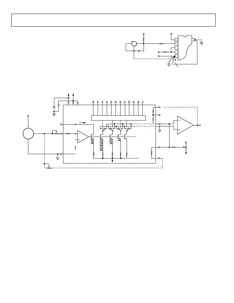
�Figure� 16.� Precision� 12-Bit� DAC�
�Rev.� C� |� Page� 10� of� 12�
�A� =� ANALOG� GROUND�
�发布紧急采购,3分钟左右您将得到回复。
相关PDF资料
MIC5801BV TR
IC DRVR LATCH 8BIT PAR IN 28PLCC
ESM06DRMH
CONN EDGECARD 12POS .156 WW
AS1322 EB
BOARD EVAL AS1322
A9CAA-0404F
FLEX CABLE - AFG04A/AF04/AFE04T
ISL60002DIH330Z-TK
IC VREF SERIES PREC 3V SOT-23-3
LQW2UASR75J00L
IND 750NH 360MA SRF 360MHZ 1008
AS1326 EB
BOARD EVAL AS1326
EGM06DRMH
CONN EDGECARD 12POS .156 WW
相关代理商/技术参数
AD581LH/+
制造商:Rochester Electronics LLC 功能描述:- Bulk
AD581S
制造商:AD 制造商全称:Analog Devices 功能描述:High Precision 10 V IC Reference
AD581SH
功能描述:IC VREF SERIES PREC 10V TO-5-3 RoHS:是 类别:集成电路 (IC) >> PMIC - 电压基准 系列:- 标准包装:2,000 系列:- 基准类型:旁路,可调节,精度 输出电压:1.24 V ~ 16 V 容差:±0.5% 温度系数:- 输入电压:1.24 V ~ 16 V 通道数:1 电流 - 阴极:100µA 电流 - 静态:- 电流 - 输出:20mA 工作温度:-40°C ~ 85°C 安装类型:通孔 封装/外壳:TO-226-3、TO-92-3(TO-226AA)成形引线 供应商设备封装:TO-92-3 包装:带卷 (TR)
AD581SH/883
制造商:未知厂家 制造商全称:未知厂家 功能描述:Voltage Reference
AD581SH/883B
制造商:Analog Devices 功能描述:V-Ref Precision 10V 10mA 3-Pin TO-5 Tube 制造商:Rochester Electronics LLC 功能描述:IC - 10V REFERENCE IC - Bulk 制造商:Analog Devices 功能描述:IC VOLT REF 10V 制造商:Analog Devices Inc. 功能描述:Voltage & Current References HI PREC 10V IC REF 制造商:Analog Devices Inc. 功能描述:Voltage & Current References IC - 10V REFERENCE IC
AD581SH/HR
制造商:未知厂家 制造商全称:未知厂家 功能描述:Voltage Reference
AD581SH1
制造商:AD 制造商全称:Analog Devices 功能描述:High Precision 10 V IC Reference
AD581T
制造商:AD 制造商全称:Analog Devices 功能描述:High Precision 10 V IC Reference